![]()
|
ece333 | doering | ece labs | ece | rhit |
|
|
ADC TheoryBoth of the converters in this project operate using the same analog hardware, which is explained below:
In essence, the analog hardware allows the digital hardware to "guess" the value of Vin and to receive a response about whether the guess is too high or too low. No information is provided whether the "guess" is correct (i.e., Vin is equal to Vc) or to what extent the "guess" is wrong. The tracking converter has a primary goal of keeping the controlled voltage Vc as close to Vin as possible at all times. If the controlled voltage is too low, then increase Vc by a unit value. If the controlled voltage is too high, then decrease Vc by a unit value. A measurement is completed just after the comparator changes states. For the most consistent results, the digital value of Vc should be saved as a measurement only for a given type of comparator transition (either low-to-high or high-to-low). The basic concept of a ramp converter is outlined below:
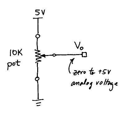
Analog Hardware Building BlocksThe analog circuit schematics are shown immediately below (click the thumbnail to see the full-size image) and are described after that:
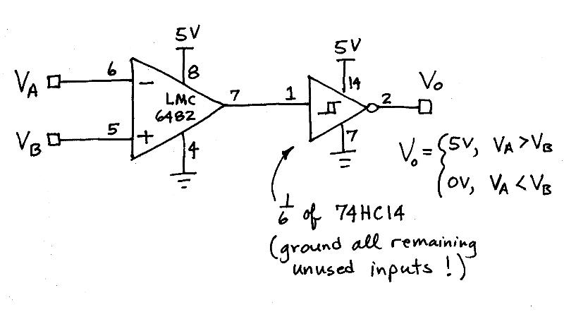
The LMC6482 rail-to-rail single-supply op amp serves as the voltage comparator, and has the following characteristics:
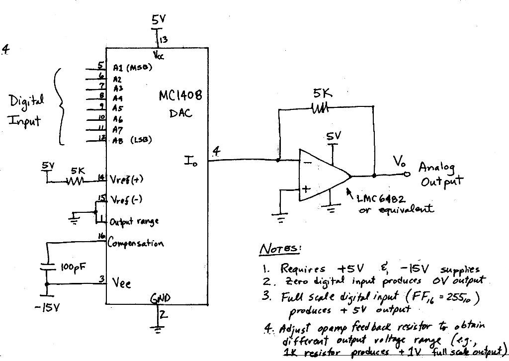
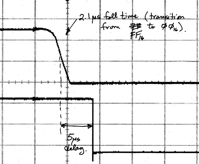
The 74HC14 hex Schmitt trigger is used between the op amp and the digital controller to ensure that the digital controller sees a clean high or low signal. When the op amp inputs become very similar (say, to within tens of microvolts), then the op amp output will not be a solid high or low voltage. The Schmitt trigger uses hysteresis to ensure that intermediate voltages get sent to either ground or Vcc. The op amp and Schmitt trigger will be collectively referred to as the "analog comparator." The MC1408 digital-to-analog converter (DAC) accepts an 8-bit digital number as input and generates a proportional analog current as output. The current is converted to a voltage by the op amp current-to-voltage converter. The device can be used as a 7-bit converter by tying the LSB low and using the upper seven bits. For example, applying 7'b0000000 will generate zero volts, applying 7'b1000000 will generate 2.5 volts, and applying 7'b1111111 will generate 5 volts. You should account for the delay associated with the DAC and analog comparator. The DAC has a measured fall time of 2.1 microseconds when the digital input transitions from FF (full scale) to 00 (zero). The analog comparator has a measured delay of 5 microseconds from input to output. Consequently, your digital system must apply input values to the DAC at a slow enough rate to assure that the analog system settles to a stable value before the digital system samples the output of the analog comparator. The measured waveforms for the preceding discussion are shown below (the top trace is the output of the DAC, and the bottom trace is the output of the comparator that is connected to the DAC):
XS-40 BoardThe XS-40 board is to be used in an "FPGA-only" mode in this project. Since you will connect your own hardware to the FPGA, you need to ensure that the pre-wired microcontroller and SRAM devices do not interfere with your analog hardware. You can accomplish this by adding two outputs to your digital system, one to hold the microcontroller reset pin in the high state (this causes all of the microcontroller pins to enter the "hi-Z" or high impedance state), and another to hold the SRAM output enable in the high state (this ensures that the SRAM outputs remain in the hi-Z state).
|
|
|