From Concept to Bitfile: Step-by-Step Instructions (Spartan 3
version)
Step 1 of 7: Create conceptual design
Digilent Spartan-3 development board
Top-side components
Bottom-side components
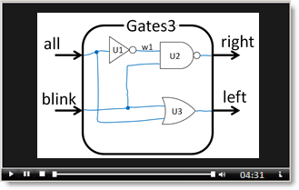
'Gates3' circuit demo
Input devices (pushbuttons)
Output devices (LEDs)
Input and output signal names
Focus on circuit inside FPGA
'Gates3' circuit schematic
Place three logic gates
Connect gates with wires
Assign reference ID to each gate
Label internal wires
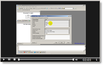
Step 2 of 7: Create new Xilinx ISE
project
Start Xilinx ISE application
Create a new project
Choose folder for project
Choose name for project
View files in project folder
Select top-level source as 'HDL'
Specify 'Spartan3' FPGA and other settings
View newly created files
Confirm location of project folder
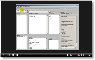
Step 3 of 7: Enter Verilog description
and testbench
Start Verilog Module Builder (vmb) application
Review vmb features
Review vmb file output types
Activate context-sensitive help
Begin with circuit schematic diagram
Enter module name
Enter descriptive text
Enter input signal names
Enter output signal names
Connect signals to output ports
Enter name of internal signal (wire)
Enter logic gate descriptions
Review auto-generated text
Save to .vmb, .v, and .txt files
Confirm files created in Xilinx project folder
Enter testbench
Review testbench structure
Save finished results
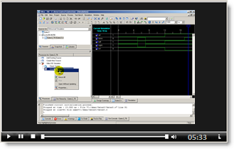
Step 4a of 7: Perform functional
verification (simulation) in Xilinx ISE or...
Return to Xilinx ISE
Add Verilog .v file to Xilinx ISE
Check syntax of testbench module
Correct syntax errors
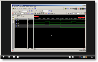
Run the ISE simulator
View simulation waveforms
Adjust waveform display order
Evaluate simulation results
Change time range to display
Iterate on design: change source code
Iterate on design: re-simulate to update waveforms
Step 4b of 7: ... in Cadence NC-Sim
Start Cadence NC-Sim simulator
Navigate to same folder as Xilinx ISE project
Create cds.lib file
Select 'verilog' design
Compile Verilog .v file
Correct syntax errors
Elaborate the design
Launch the simulator
Select waveforms to display
Run the simulation
Display entire time range
Evaluate the simulation results
Iterate on the design: Change Verilog .v file
Iterate on the design: Re-run the simulator
Adjust waveform order
Adjust time range (zoom, region select)
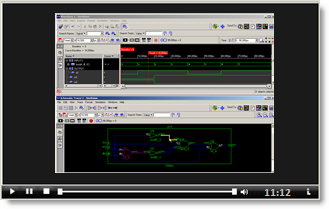
View Verilog .v file as a circuit diagram
Step 5 of 7: Synthesize design to
bitstream file
Return to Xilinx ISE
Review signal names and connected devices
Open UCF generator spreadsheet
Associate signal names with devices
Copy UCF text from spreadsheet
Paste text into Xilinx ISE constraints file
Set startup clock to JTAG
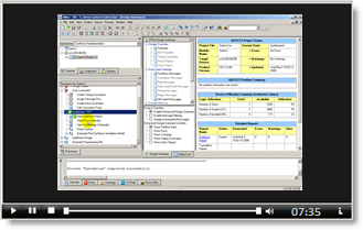
Synthesize the design
View synthesized design as RTL schematic
View synthesized design as technology schematic
Implement the design
Review device utilization
Confirm correct pin assignment
Generate .bit file
Steps 6 and 7 of 7: Download bitstream
file to FPGA; Test the design
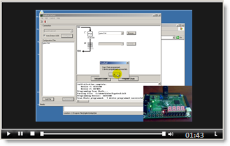
Launch 'ExPort' application
Confirm 'auto-detect' enabled
Locate .bit file
Initial board communications
De-select ROM
Select .bit file
Download .bit file to FPGA
Test the design
"Inverter Demo" -- Same as the
7-step process above, but with the all-in-one bundled software
Primary Differences:
- Slight change in the Xilinx ISE project setup
- Need to correctly designate the "top-level" module (new version
defaults to testbench module)
- Need to create the UCF file from a text editor, and then add it to the
project
- Must move the .bit file out of the virtual machine to the Windows file
system using SecureFX
- The Digilent Adept application has a different (improved) look and
feel
Cadence
Simulation Techniques
Circuit to be simulated
Verilog translation of circuit
Testbench for circuit
"for-loop" technique
to test all input combinations
Start Cadence NC-Launch
Set design
directory
Create CDS.LIB file
Compile Verilog modules
Elaborate testbench module
Launch simulator
Select waveforms to display
Run
simulator
Show entire simulation in one screen
Adjust waveform position
Adjust cursor position
Modify a source file
Re-simulate the modified
source file
Revert to original circuit
Organize waveforms into related
groups
Convert related signals to a bus
Select radix for bus display
Delete a waveform trace
View Verilog description as a schematic diagram
Compare Cadence schematic to original
Use "cursor stroke" to view full
schematic
Cross-probe between waveform display and schematic diagram
Cross-probe between schematic and source files
Make hardcopy of waveform
traces
Print schematic diagram

 .
.