

Operational amplifier applications
From Wikipedia, the free encyclopedia
This article illustrates some typical applications of operational amplifiers. A simplified schematic notation is used, and the reader is reminded that many details such as device selection and power supply connections are not shown.
[edit] Practical considerations
[edit] Input offset problems
It is important to note that the equations shown below, pertaining to each type of circuit, assume that an ideal op amp is used. Those interested in construction of any of these circuits for practical use should consult a more detailed reference. See the External links and Further reading sections.
Resistors used in practical solid-state op-amp circuits are typically in the kΩ range. Resistors much greater than 1 MΩ cause excessive thermal noise and make the circuit operation susceptible to significant errors due to bias or leakage currents.
Practical operational amplifiers draw a small current from each of their inputs due to bias requirements and leakage. These currents flow through the resistances connected to the inputs and produce small voltage drops across those resistances. In AC signal applications this seldom matters. If high-precision DC operation is required, however, these voltage drops need to be considered. The design technique is to try to ensure that these voltage drops are equal for both inputs, and therefore cancel. If these voltage drops are equal and the common-mode rejection ratio of the operational amplifier is good, there will be considerable cancellation and improvement in DC accuracy.
If the input currents into the operational amplifier are equal, to reduce offset voltage the designer must ensure that the DC resistance looking out of each input is also matched. In general input currents differ, the difference being called the input offset current, Ios. Matched external input resistances Rin will still produce an input voltage error of Rin·Ios . Most manufacturers provide a method for tuning the operational amplifier to balance the input currents (e.g., "offset null" or "balance" pins that can interact with an external voltage source attached to a potentiometer). Otherwise, a tunable external voltage can be added to one of the inputs in order to balance out the offset effect. In cases where a design calls for one input to be short-circuited to ground, that short circuit can be replaced with a variable resistance that can be tuned to mitigate the offset problem.
Note that many operational amplifiers that have MOSFET-based input stages have input leakage currents that will truly be negligible to most designs.
[edit] Power supply effects
Although the power supplies are not shown in the operational amplifier designs below, they can be critical in operational amplifier design.
Power supply imperfections (e.g., power signal ripple, non-zero source impedance) may lead to noticeable deviations from ideal operational amplifier behavior. For example, operational amplifiers have a specified power supply rejection ratio that indicates how well the output can reject signals that appear on the power supply inputs. Power supply inputs are often noisy in large designs because the power supply is used by nearly every component in the design, and inductance effects prevent current from being instantaneously delivered to every component at once. As a consequence, when a component requires large injections of current (e.g., a digital component that is frequently switching from one state to another), nearby components can experience sagging at their connection to the power supply. This problem can be mitigated with copious use of bypass capacitors placed connected across each power supply pin and ground. When bursts of current are required by a component, the component can bypass the power supply by receiving the current directly from the nearby capacitor (which is then slowly charged by the power supply).
Additionally, current drawn into the operational amplifier from the power supply can be used as inputs to external circuitry that augment the capabilities of the operational amplifier. For example, an operational amplifier may not be fit for a particular high-gain application because its output would be required to generate signals outside of the safe range generated by the amplifier. In this case, an external push–pull amplifier can be controlled by the current into and out of the operational amplifier. Thus, the operational amplifier may itself operate within its factory specified bounds while still allowing the negative feedback path to include a large output signal well outside of those bounds.[1]
[edit] Circuit applications
[edit] Comparator

Compares two voltages and switches its output to indicate which voltage is larger.
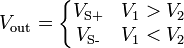
(where Vs is the supply voltage and the opamp is powered by + Vs and − Vs.)
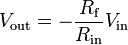
[edit] Inverting amplifier

An inverting amplifier uses negative feedback to invert and amplify a voltage. The Rf resistor allows some of the output signal to be returned to the input. Since the output is 180° out of phase, this amount is effectively subtracted from the input, thereby reducing the input into the operational amplifier. This reduces the overall gain of the amplifier and is dubbed negative feedback.[2]
- Zin = Rin (because V − is a virtual ground)
- A third resistor, of value
 , added between the non-inverting input and ground, while not necessary, minimizes errors due to input bias currents.
The gain of the amplifier is determined by the ratio of Rf to Rin. That is:

The presence of the negative sign is a convention indicating that the output is inverted. For example, if Rf is 10,000 Ω and Rin is 1,000 Ω, then the gain would be -10000Ω/1000Ω, which is -10. [4]
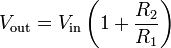
[edit] Non-inverting amplifier

Amplifies a voltage (multiplies by a constant greater than 1)
- Input impedance

- The input impedance is at least the impedance between non-inverting ( + ) and inverting ( − ) inputs, which is typically 1 MΩ to 10 TΩ, plus the impedance of the path from the inverting ( − ) input to ground (i.e., R1 in parallel with R2).
- Because negative feedback ensures that the non-inverting and inverting inputs match, the input impedance is actually much higher.
- Although this circuit has a large input impedance, it suffers from error of input bias current.
- The non-inverting ( + ) and inverting ( − ) inputs draw small leakage currents into the operational amplifier.
- These input currents generate voltages that act like unmodeled input offsets. These unmodeled effects can lead to noise on the output (e.g., offsets or drift).
- Assuming that the two leaking currents are matched, their effect can be mitigated by ensuring the DC impedance looking out of each input is the same.
- The voltage produced by each bias current is equal to the product of the bias current with the equivalent DC impedance looking out of each input. Making those impedances equal makes the offset voltage at each input equal, and so the non-zero bias currents will have no impact on the difference between the two inputs.
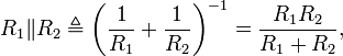
- A resistor of value
- which is the equivalent resistance of R1 in parallel with R2, between the Vin source and the non-inverting ( + ) input will ensure the impedances looking out of each input will be matched.
- The matched bias currents will then generate matched offset voltages, and their effect will be hidden to the operational amplifier (which acts on the difference between its inputs) so long as the CMRR is good.
- Very often, the input currents are not matched.
- Most operational amplifiers provide some method of balancing the two input currents (e.g., by way of an external potentiometer).
- Alternatively, an external offset can be added to the operational amplifier input to nullify the effect.
- Another solution is to insert a variable resistor between the Vin source and the non-inverting ( + ) input. The resistance can be tuned until the offset voltages at each input are matched.
- Operational amplifiers with MOSFET-based input stages have input currents that are so small that they often can be neglected.
[edit] Differential amplifier

The circuit shown is used for finding the difference of two voltages each multiplied by some constant (determined by the resistors).
The name "differential amplifier" should not be confused with the "differentiator", also shown on this page.
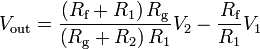
- Differential Zin (between the two input pins) = R1 + R2 (Note: this is approximate)
For common-mode rejection, anything done to one input must be done to the other. The addition of a compensation capacitor in parallel with Rf, for instance, must be balanced by an equivalent capacitor in parallel with Rg.
The "instrumentation amplifier", which is also shown on this page, is another form of differential amplifier that also provides high input impedance.
Whenever  and
and  , the differential gain is
 and
and 
When  and
and  the differential gain is A = 1 and the circuit acts as a differential follower:
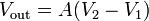
[edit] Voltage follower

Used as a buffer amplifier to eliminate loading effects (e.g., connecting a device with a high source impedance to a device with a low input impedance).

 (realistically, the differential input impedance of the op-amp itself, 1 MΩ to 1 TΩ)
Due to the strong (i.e., unity gain) feedback and certain non-ideal characteristics of real operational amplifiers, this feedback system is prone to have poor stability margins. Consequently, the system may be unstable when connected to sufficiently capacitive loads. In these cases, a lag compensation network (e.g., connecting the load to the voltage follower through a resistor) can be used to restore stability. The manufacturer data sheet for the operational amplifier may provide guidance for the selection of components in external compensation networks. Alternatively, another operational amplifier can be chosen that has more appropriate internal compensation.
[edit] Summing amplifier

A summing amplifer sums several (weighted) voltages:
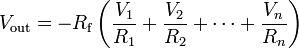
- When
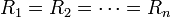 , and Rf independent
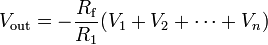
- When


- Output is inverted
- Input impedance of the nth input is Zn = Rn (V − is a virtual ground)
[edit] Integrator

Integrates the (inverted) signal over time
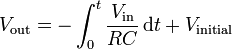
(where Vin and Vout are functions of time, Vinitial is the output voltage of the integrator at time t = 0.)
- Note that this can also be viewed as a low-pass electronic filter. It is a filter with a single pole at DC (i.e., where ω = 0) and gain.
- There are several potential problems with this circuit.
- It is usually assumed that the input Vin has zero DC component (i.e., has a zero average value). Otherwise, unless the capacitor is periodically discharged, the output will drift outside of the operational amplifier's operating range.
- Even when Vin has no offset, the leakage or bias currents into the operational amplifier inputs can add an unexpected offset voltage to Vin that causes the output to drift. Balancing input currents and replacing the non-inverting ( + ) short-circuit to ground with a resistor with resistance R can reduce the severity of this problem.
- Because this circuit provides no DC feedback (i.e., the capacitor appears like an open circuit to signals with ω = 0), the offset of the output may not agree with expectations (i.e., Vinitial may be out of the designer's control with the present circuit).
- Many of these problems can be made less severe by adding a large resistor RF in parallel with the feedback capacitor. At significantly high frequencies, this resistor will have negligible effect. However, at low frequencies where there are drift and offset problems, the resistor provides the necessary feedback to hold the output steady at the correct value. In effect, this resistor reduces the DC gain of the "integrator" – it goes from infinite to some finite value RF / R.
[edit] Differentiator

Differentiates the (inverted) signal over time.

- Note that this can also be viewed as a high-pass electronic filter. It is a filter with a single zero at DC (i.e., where ω = 0) and gain. The high pass characteristics of a differentiating amplifier can lead to unstable behavior when the circuit is used in an analog servo loop. For this reason the system function would be re-formulated to use integrators.
[edit] Instrumentation amplifier

Combines very high input impedance, high common-mode rejection, low DC offset, and other properties used in making very accurate, low-noise measurements
- Is made by adding a non-inverting buffer to each input of the differential amplifier to increase the input impedance.
[edit] Schmitt trigger
A bistable multivibrator implemented as a comparator with hysteresis.

In this configuration, the input voltage is applied through the resistor R1 (which may be the source internal resistance) to the non-inverting input and the inverting input is grounded or referenced. The hysteresis curve is non-inverting and the switching thresholds are  where Vsat is the greatest output magnitude of the operational amplifier.

Alternatively, the input source and the ground may be swapped. Now the input voltage is applied directly to the inverting input and the non-inverting input is grounded or referenced. The hysteresis curve is inverting and the switching thresholds are 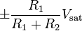 . Such a configuration is used in the relaxation oscillator shown below.
[edit] Relaxation oscillator

By using an RC network to add slow negative feedback to the inverting Schmitt trigger, a relaxation oscillator is formed. The feedback through the RC network causes the Schmitt trigger output to oscillate in an endless symmetric square wave (i.e., the Schmitt trigger in this configuration is an astable multivibrator).
[edit] Inductance gyrator

Simulates an inductor (i.e., provides inductance without the use of a possibly costly inductor). The circuit exploits the fact that the current flowing through a capacitor behaves through time as the voltage across an inductor. The capacitor used in this circuit is smaller than the inductor it simulates and its capacitance is less subject to changes in value due to environmental changes.
[edit] Zero level detector
Voltage divider reference
- Zener sets reference voltage
[edit] Negative impedance converter (NIC)

Creates a resistor having a negative value for any signal generator
- In this case, the ratio between the input voltage and the input current (thus the input resistance) is given by:
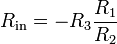
In general, the components R1, R2, and R3 need not be resistors; they can be any component that can be described with an impedance.
[edit] Wien bridge oscillator

Produces a pure sine wave.
[edit] Precision rectifier

The voltage drop VF across the forward biased diode in the circuit of a passive rectifier is undesired. In this active version, the problem is solved by connecting the diode in the negative feedback loop. The op-amp compares the output voltage across the load with the input voltage and increases its own output voltage with the value of VF. As a result, the voltage drop VF is compensated and the circuit behaves as an ideal (super) diode with VF = 0 V.
The circuit has speed limitations at high frequency because of the slow negative feedback.
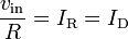
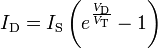
[edit] Logarithmic output

- The relationship between the input voltage vin and the output voltage vout is given by:
- where IS is the saturation current and VT is the thermal voltage.
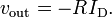
- If the operational amplifier is considered ideal, the negative pin is virtually grounded, so the current flowing into the resistor from the source (and thus through the diode to the output, since the op-amp inputs draw no current) is:
- where ID is the current through the diode. As known, the relationship between the current and the voltage for a diode is:
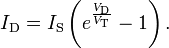
- This, when the voltage is greater than zero, can be approximated by:

- Putting these two formulae together and considering that the output voltage is the negative of the voltage across the diode (Vout = − VD), the relationship is proven.
Note that this implementation does not consider temperature stability and other non-ideal effects.
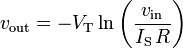
[edit] Exponential output

- The relationship between the input voltage vin and the output voltage vout is given by:
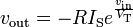
where IS is the saturation current and VT is the thermal voltage.
- Considering the operational amplifier ideal, then the negative pin is virtually grounded, so the current through the diode is given by:
when the voltage is greater than zero, it can be approximated by:
The output voltage is given by:
[edit] Other applications
- audio and video pre-amplifiers and buffers
- voltage comparators
- differential amplifiers
- differentiators and integrators
- filters
- precision rectifiers
- voltage regulator and current regulator
- analog-to-digital converter
- digital-to-analog converter
- voltage clamps
- oscillators and waveform generators
- Schmitt trigger
- Gyrator
- Comparator
- Active filter
- Analog computer
- Capacitance multiplier
[edit] See also
- Operational amplifier
- Current-feedback operational amplifier
- Operational transconductance amplifier
- Frequency compensation
- George A. Philbrick
[edit] References
- ^ Paul Horowitz and Winfield Hill, The Art of Electronics. 2nd ed. Cambridge University Press, Cambridge, 1989 ISBN 0-521-37095-7
- ^ Basic Electronics Theory, Delton T. Horn, 4th ed. McGraw-Hill Professional, 1994, p.342-343.
- ^ Malmstadt, Enke and Crouch, Electronics and Instrumentation for Scientists, The Benjamin/Cummings Publishing Company, Inc., 1981, ISBN 0-8053-6917-1, Chapter 5. pp 118.
- ^ Basic Electronics Theory, Delton T. Horn, 4th ed. McGraw-Hill Professional, 1994, p.342-343.
[edit] Further reading
- Paul Horowitz and Winfield Hill, The Art of Electronics. 2nd ed. Cambridge University Press, Cambridge, 1989 ISBN 0-521-37095-7
- Sergio Franco, Design with Operational Amplifiers and Analog Integrated Circuits, 3rd ed., McGraw-Hill, New York, 2002 ISBN 0-07-232084-2
[edit] External links
| The Wikibook Electronics has a page on the topic of |
| The Wikibook Circuit Idea has a page on the topic of |
- Introduction to op-amp circuit stages, second order filters, single op-amp bandpass filters, and a simple intercom
- Op Amps for EveryonePDF (1.96 MiB)
- Single supply op-amp circuit collectionPDF (163 KiB)
- Op-amp circuit collectionPDF (962 KiB)
- A Collection of Amp ApplicationsPDF (1.06 MiB) – Analog Devices Application note
- Basic OpAmp ApplicationsPDF (173 KiB)
- Handbook of operational amplifier applicationsPDF (2.00 MiB) – Texas Instruments Application note
- Low Side Current Sensing Using Operational Amplifiers
- Log/anti-log generators, cube generator, multiply/divide ampPDF (165 KiB)
- Logarithmically variable gain from a linear variable component
- Impedance and admittance transformations using operational amplifiers by D. H. Sheingold